- 您现在的位置:买卖IC网 > Sheet目录3855 > PIC16C62B-20/SS (Microchip Technology)IC MCU OTP 2KX14 PWM 28SSOP
PIC16C62B/72A
DS35008B-page 102
Preliminary
1998 Microchip Technology Inc.
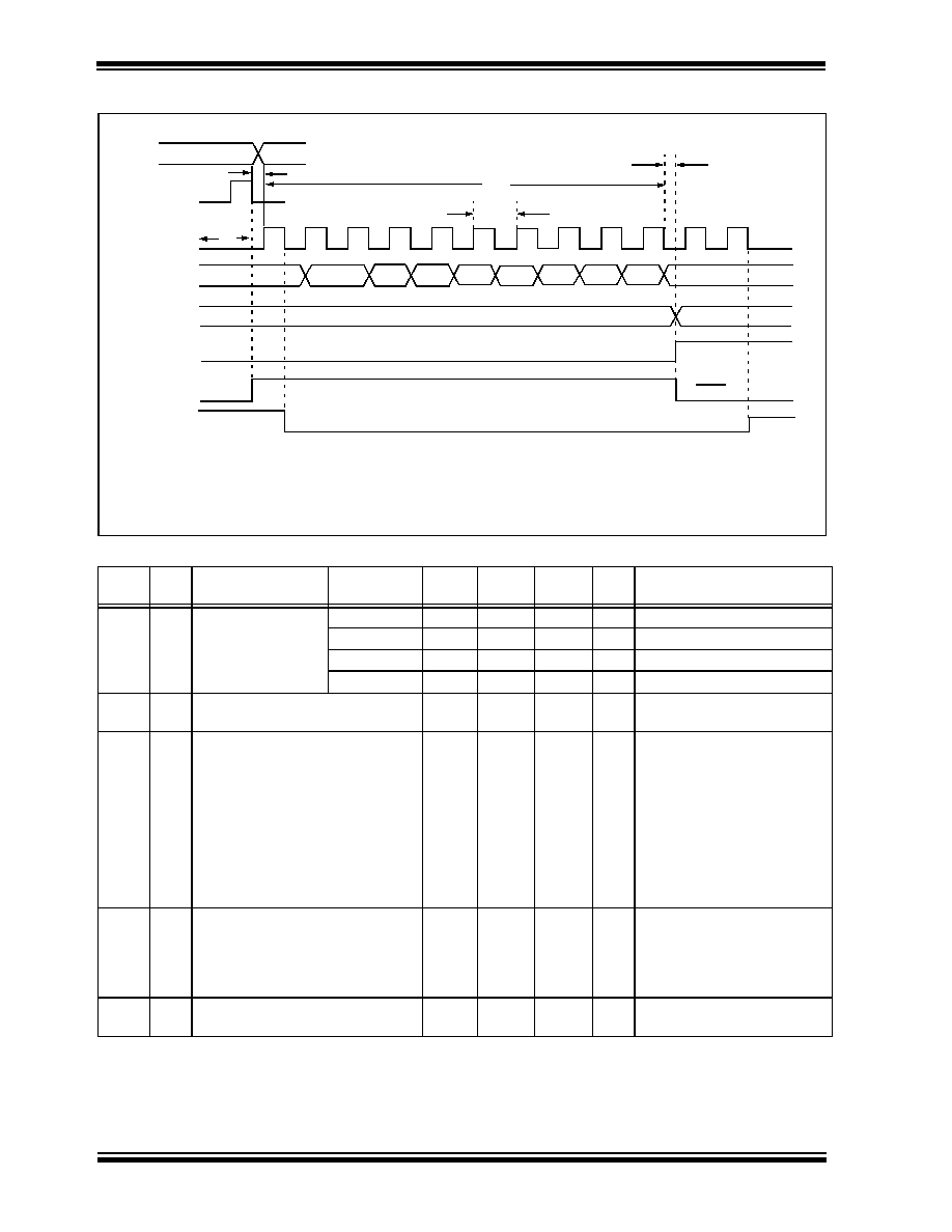
FIGURE 13-17: A/D CONVERSION TIMING
TABLE 13-14: A/D CONVERSION REQUIREMENTS
Param
No.
Sym
Characteristic
Min
Typ
Max
Unit
s
Conditions
130
TAD
A/D clock period
PIC16CXX
1.6
——
sTOSC based, VREF ≥ 3.0V
PIC16LCXX
2.0
—
sTOSC based, VREF full range
PIC16CXX
2.0
4.0
6.0
sA/D RC Mode
PIC16LCXX
3.0
6.0
9.0
sA/D RC Mode
131
TCNV Conversion time (not including S/H
time) (Note 1)
11
—
11
TAD
132
TACQ Acquisition time
Note 2
5*
20
—
s
s The minimum time is the
amplifier settling time. This
may be used if the "new" input
voltage has not changed by
more than 1 LSb (i.e., 20.0 mV
@ 5.12V) from the last sam-
pled voltage (as stated on
CHOLD).
134
TGO
Q4 to A/D clock start
—
TOSC/2
—
If the A/D clock source is
selected as RC, a time of TCY
is added before the A/D clock
starts. This allows the SLEEP
instruction to be executed.
135
Tswc Switching from convert
→ sample
time
1.5
—
TAD
* These parameters are characterized but not tested.
Data in “Typ” column is at 5V, 25
°C unless otherwise stated. These parameters are for design guidance only
and are not tested.
Note 1: ADRES register may be read on the following TCY cycle.
2: See Section 9.1 for min conditions.
131
130
132
BSF ADCON0, GO
Q4
A/D CLK
A/D DATA
ADRES
ADIF
GO
SAMPLE
OLD_DATA
SAMPLING STOPPED
DONE
NEW_DATA
(Tosc/2) (1)
7
6
5
432
1
0
Note 1: If the A/D clock source is selected as RC, a time of TCY is added before the A/D clock starts. This
allows the SLEEP instruction to be executed.
1 TCY
134
发布紧急采购,3分钟左右您将得到回复。
相关PDF资料
PIC16LC711-04I/SO
IC MCU OTP 1KX14 A/D 18SOIC
PIC18F66J90-I/PT
IC PIC MCU FLASH 64KB 64-TQFP
ATMEGA32L-8AC
IC AVR MCU 32K LV 8MHZ COM44TQFP
DSPIC30F2012-30I/SP
IC DSPIC MCU/DSP 12K 28DIP
PIC18LF2321-I/ML
IC PIC MCU FLASH 4KX16 28QFN
PIC18F4321-I/P
IC PIC MCU FLASH 4KX16 40DIP
ATMEGA32L-8MC
IC AVR MCU 32K LV 8MHZ COM 44QFN
PIC18F2450-I/SP
IC PIC MCU FLASH 8KX16 28DIP
相关代理商/技术参数
PIC16C62B-20E/SO
功能描述:8位微控制器 -MCU 3.5KB 128 RAM 22 I/O RoHS:否 制造商:Silicon Labs 核心:8051 处理器系列:C8051F39x 数据总线宽度:8 bit 最大时钟频率:50 MHz 程序存储器大小:16 KB 数据 RAM 大小:1 KB 片上 ADC:Yes 工作电源电压:1.8 V to 3.6 V 工作温度范围:- 40 C to + 105 C 封装 / 箱体:QFN-20 安装风格:SMD/SMT
PIC16C62B-20E/SP
功能描述:8位微控制器 -MCU 3.5KB 128 RAM 22 I/O RoHS:否 制造商:Silicon Labs 核心:8051 处理器系列:C8051F39x 数据总线宽度:8 bit 最大时钟频率:50 MHz 程序存储器大小:16 KB 数据 RAM 大小:1 KB 片上 ADC:Yes 工作电源电压:1.8 V to 3.6 V 工作温度范围:- 40 C to + 105 C 封装 / 箱体:QFN-20 安装风格:SMD/SMT
PIC16C62B-20E/SS
功能描述:8位微控制器 -MCU 3.5KB 128 RAM 22 I/O RoHS:否 制造商:Silicon Labs 核心:8051 处理器系列:C8051F39x 数据总线宽度:8 bit 最大时钟频率:50 MHz 程序存储器大小:16 KB 数据 RAM 大小:1 KB 片上 ADC:Yes 工作电源电压:1.8 V to 3.6 V 工作温度范围:- 40 C to + 105 C 封装 / 箱体:QFN-20 安装风格:SMD/SMT
PIC16C62B-20I/ML
功能描述:8位微控制器 -MCU 3.5KB 128 RAM 22 I/O RoHS:否 制造商:Silicon Labs 核心:8051 处理器系列:C8051F39x 数据总线宽度:8 bit 最大时钟频率:50 MHz 程序存储器大小:16 KB 数据 RAM 大小:1 KB 片上 ADC:Yes 工作电源电压:1.8 V to 3.6 V 工作温度范围:- 40 C to + 105 C 封装 / 箱体:QFN-20 安装风格:SMD/SMT
PIC16C62B-20I/SO
功能描述:8位微控制器 -MCU 3.5KB 128 RAM 22 I/O RoHS:否 制造商:Silicon Labs 核心:8051 处理器系列:C8051F39x 数据总线宽度:8 bit 最大时钟频率:50 MHz 程序存储器大小:16 KB 数据 RAM 大小:1 KB 片上 ADC:Yes 工作电源电压:1.8 V to 3.6 V 工作温度范围:- 40 C to + 105 C 封装 / 箱体:QFN-20 安装风格:SMD/SMT
PIC16C62B-20I/SO
制造商:Microchip Technology Inc 功能描述:8BIT CMOS MCU SMD 16C62 SOIC28
PIC16C62B-20I/SP
功能描述:8位微控制器 -MCU 3.5KB 128 RAM 22 I/O RoHS:否 制造商:Silicon Labs 核心:8051 处理器系列:C8051F39x 数据总线宽度:8 bit 最大时钟频率:50 MHz 程序存储器大小:16 KB 数据 RAM 大小:1 KB 片上 ADC:Yes 工作电源电压:1.8 V to 3.6 V 工作温度范围:- 40 C to + 105 C 封装 / 箱体:QFN-20 安装风格:SMD/SMT
PIC16C62B-20I/SP
制造商:Microchip Technology Inc 功能描述:IC 8BIT CMOS MCU 16C62 SDIL28